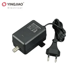
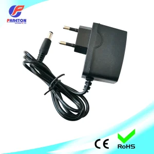
Explore our premium, certified power conversion solutions engineered for efficiency, thermal resilience, and ultra-compact form factors.
Established in 2004 in the technology hub of Shenzhen, ShenZhen JDI Power Supply Co., Ltd. is a distinguished national high-tech enterprise and a New Third Board listed entity. Spanning a modern 6,000 square meter production base, we combine state-of-the-art facilities with cutting-edge engineering capabilities to supply global brands with highly reliable, compact power conversion solutions.
Our research and development team, consisting of over 20 veteran engineers, is directed by a lead scientist with 27 years of pioneering experience in power electronics. This deep expertise empowers us to develop over 1,000 distinct products tailored for high-stakes applications including medical systems, smart home automation, security electronics, AV products, and heavy industrial instrumentation.
Pioneering the next generation of power electronics with semiconductor innovations and smart topological designs.
By shifting from conventional silicon switches to Gallium Nitride (GaN) and Silicon Carbide (SiC) semiconductors, we achieve switching frequencies exceeding 500kHz. This dramatically reduces size while pushing energy efficiency beyond 95%, allowing cooler operations in tightly sealed compact housings.
Conventional wire-wound transformers are being replaced by multilayer planar transformers integrated directly into the PCB layout. This structure guarantees reproducible parasitic elements, slashes electromagnetic interference (EMI) profiles, and minimizes vertical stack height for low-profile industrial chassis.
Utilizing microcontrollers for real-time monitoring of voltage loop parameters allows us to deploy predictive transient algorithms. Digital control ensures outstanding dynamic response, enables localized diagnostic telemetry via PMBus, and guarantees long-term stability against component aging.
Delivering high-reliability power grids designed to operate optimally within demanding medical, industrial, and consumer environments.
Compliance with the strict IEC/EN 60601-1 3rd Edition framework is mandatory. Our medical-grade compact adaptors offer 2xMOPP (Means of Patient Protection) isolation, extremely low leakage currents (<100μA), and exceptional electromagnetic compatibility designed for diagnostic devices, active patient monitoring equipment, and therapeutic tools.
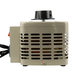
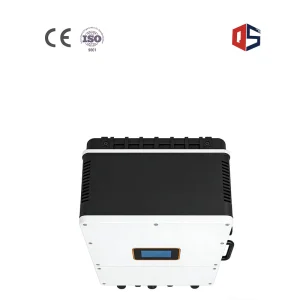
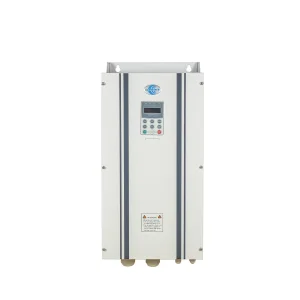
Designed to withstand severe industrial environments. Implementing dynamic VFD technologies and high-wattage step-down isolation allows our systems to operate flawlessly within a wider thermal window (-40°C to +85°C) and provide heavy-duty resistance against mains surges and physical vibrations.
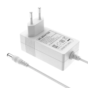
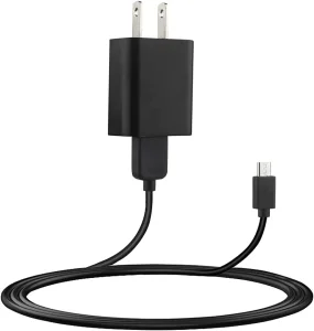
Optimized for IoT frameworks, smart home lighting, and mass-market consumer devices. Our slim wall adapters and universal charging modules focus on maximizing power delivery while minimizing stand-by energy draw, exceeding the demanding guidelines set by CoC Tier 2 and DoE Level VI.
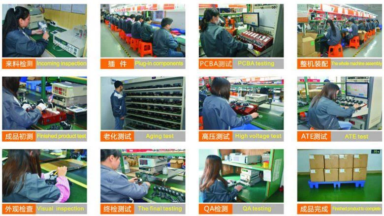
The Shenzhen JDI factory operates at the interface of modern automation and lean manufacturing. Through extensive integrations of Smart MES (Manufacturing Execution Systems), our surface-mount (SMT) and automated wave soldering processes achieve consistent, traceably high yields. By automating components routing and soldering, we eliminate human errors and maintain high precision across multi-million unit batches.
Supply chain resilience is anchored on our localized logistics network. Located in Shenzhen, we access the world's most concentrated silicon, magnetic core, and PCB substrate manufacturing ecosystem. This proximity cuts design loops, provides immediate supply redundancy, and shields global clients from sudden logistical disruptions.
Whether dealing with critical component allocations or demanding surge orders, our production flexibility guarantees rapid raw material access and minimal delivery lead times.
Every single PCB assembly passes through AOI checks to scan for soldering and placement irregularities.
Products are subjected to high-temperature, full-load burn-in cycles to filter out infant mortality failures.
Comprehensive electrical test routines evaluate overvoltage, overcurrent, short circuit, and efficiency performance automatically.
Navigating the complex landscape of global certifications to ensure smooth custom clearance and regional safety compliance.
To assist our international buyers, our power solutions carry full certifications for global target markets. By executing internal pre-compliance testing within our advanced testing laboratory, we speed up regulatory cycles and guarantee seamless import workflows.
Our components comply with rigorous worldwide safety regulations, eliminating the risk of border delays or compliance issues.
Meeting global energy consumption targets with low-energy dissipation topologies and environmental checks.
Reliability is not an afterthought—it is designed directly into the product. Our internal laboratory utilizes advanced testing infrastructure to evaluate prototypes and production batches against extreme stressors:
Understanding and fulfilling the strategic procurement targets of Tier-1 OEMs, distributors, and global enterprises.
We work directly with supply chains to optimize manufacturing processes. By implementing automated assembly lines and maintaining long-standing raw material contracts, we deliver high margins for distributors and affordable costs for large-scale OEMs.
From initial design sketches to structural engineering, custom PCB layouts, electrical simulations, and thermal profiling, our engineering division supports your product development team throughout the entire cycle.
We optimize warehousing and production tracking to secure stable lead times. Backed by extensive output capacities in our Shenzhen complex, we fulfill repeat container-load orders without compromising quality.
Providing technical answers to help buyers evaluate quality, efficiency, and engineering capabilities.
For custom ODM projects, the design cycle requires approximately 3 to 4 weeks to complete the initial layout, simulation, and working prototypes. Once the client approves these samples, safety certifications (UL, CE, PSE) require an additional 4 to 8 weeks depending on the target region. Mass production setup normally takes 4 weeks from order confirmation.
Our medical adapters are engineered according to the IEC/EN 60601-1 standard. They feature dual-level galvanic isolation (2xMOPP) and a safe physical isolation distance between primary and secondary circuits. Additionally, each batch undergoes strict leakage current testing to verify patient-side isolation safety.
We use a combination of automated testing setups. Components undergo rigorous stress analysis (evaluating junction temperatures and voltage stress limits), followed by HALT (Highly Accelerated Life Testing) to identify structural failure limits. Additionally, we run continuous high-temperature aging chambers under 100% load configurations on all production series.
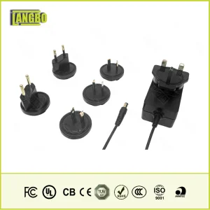
Yes. We provide compliance adaptions tailored for markets across North America, Europe, the UK, Japan, Korea, Australia, China, Brazil, and Argentina. This includes modifications for local plugs (US, EU, UK, AU, CN) as well as compliance with safety regulations like PSE, KC, CCC, CE, GS, UL, and SAA.
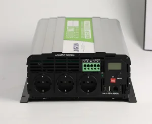
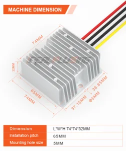
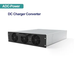
Heavy-duty, high-efficiency, and isolated voltage regulation converters designed for commercial architectures.