How to Minimize Power Loss During AC-DC Conversion? This question matters wherever electricity enters a real product. A phone charger, server supply, or industrial drive can waste energy through heat, switching losses, conduction resistance, magnetic losses, and standby consumption. The losses may seem small on a schematic. They become obvious when a metal enclosure feels hot, a fan runs continuously, or a power meter records unnecessary consumption.
Dr. Alex Lidow, a leading power-electronics researcher and co-founder of Efficient Power Conversion, has said, “GaN is not a magic bullet.” That warning deserves attention. Gallium nitride devices can reduce switching losses and support higher frequencies, but layout, gate control, dead time, thermal design, and operating conditions still determine the result. A poorly designed GaN converter can perform worse than a carefully optimized silicon design. Reality is less tidy.
This guide examines practical methods to minimize power loss during AC-DC conversion. It considers rectifier selection, power-factor correction, transformer design, switching frequency, soft-switching methods, cooling, and control strategies. Measurement is essential. Compare input and output power at light, medium, and full loads. Record temperatures near the bridge rectifier, switching devices, transformer, and output diodes. Small details matter.
There is no perfect converter. Every improvement introduces trade-offs. Higher frequency can reduce magnetic size but increase switching loss. Larger components may lower resistance but raise cost and volume. Even experienced designers miss something occasionally. A reliable design therefore combines calculations, simulation, laboratory measurements, and honest review of unexpected results.
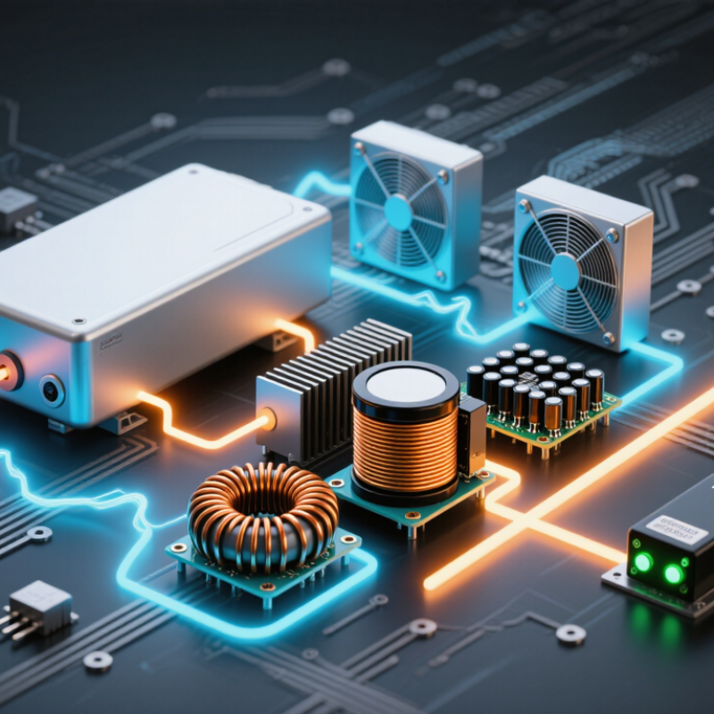
How to Minimize Power Loss During AC DC Conversion?
Understanding Where Power Loss Occurs During AC-DC Conversion
AC to DC conversion loses power at several points, not one mysterious location. The transformer or input inductor warms through copper resistance and core losses. Rectifier diodes add a forward-voltage drop, turning current into unwanted heat. At high load, even a small voltage drop matters. A 12-volt output carrying 10 amps can lose 14 watts through two 0.7-volt diode drops. That is significant heat.
Switch-mode stages introduce different losses. MOSFET conduction, switching transitions, gate drive circuits, and magnetic hysteresis all consume energy. Capacitor equivalent series resistance also creates ripple-related heating. PCB traces contribute loss when they are narrow or unnecessarily long. Under light load, control circuits and bleeder resistors may dominate. A thermal camera can reveal hot spots near rectifiers, inductors, and crowded current paths. Infrared readings still need care. Shiny surfaces can give misleading temperatures.
Measure input and output power across the full load range. Use calibrated meters, not one quick reading. Synchronous rectification can reduce diode losses, while lower-resistance switching devices reduce conduction loss. Better airflow, thicker copper, and shorter current loops also help. Keep sufficient voltage margin and check ripple under transient loads. I would not optimize only for peak efficiency. My first prototype once ran efficiently but overheated during repeated startups. That result needed more reflection. Designing for stable temperatures often matters more than achieving one impressive test number.
During AC-DC conversion, losses often begin before switching starts. Choose rectifiers by operating current, reverse voltage, recovery behavior, and temperature. A diode bridge is simple, but its forward drop wastes power continuously. Synchronous rectification can reduce conduction loss at low output voltages, though timing control adds risk.
Measure under real load.
The U.S. Department of Energy has estimated annual distribution-transformer losses near 60 billion kWh in the United States. (DOE, Energy Savings Potential and RD&D Opportunities for Commercial Building Appliances, 2014.)
Transformer selection is not paperwork.
Select transformers for both no-load and load losses. A lightly loaded unit can waste energy all night through core magnetization. European Commission studies have placed European transformer losses around 93 TWh annually, equal to roughly 2.5% of electricity use. (Ecodesign Preparatory Study on Transformers, 2015.)
For switching devices, compare conduction loss, switching energy, gate-drive demand, and leakage at the actual frequency. Silicon devices remain practical, while wide-bandgap devices may reduce switching losses. Layout and control quality decide whether those gains survive.
Keep copper paths short and inspect ringing with an oscilloscope. Datasheet efficiency is not field efficiency.
A balanced design usually wins.
Efficient AC-DC conversion begins with controlling current paths, not simply choosing lower-resistance components. During bench testing, I measure voltage and current at the input, switching node, and output. These readings reveal losses that simulations may overlook.
Conduction loss rises with current and resistance. Keep copper paths short, wide, and thermally supported. Select rectifiers and switching devices with suitable forward voltage or on-resistance. A smaller device may appear economical, but its heat can increase resistance and create further loss. Thermal design matters.
Switching loss needs careful timing. Excessive switching frequency increases transition losses, while a low frequency may require larger magnetic components. Adjust gate drive strength, dead time, and snubber values after observing real waveforms. Use an oscilloscope with proper probing. Poor probe grounding can produce misleading spikes.
Layout is often underestimated. Keep high di/dt loops compact, place bypass capacitors close to switching devices, and separate noisy power paths from control signals. Soft-switching methods can reduce overlap between voltage and current, but they also add design complexity. This trade-off deserves testing.
Small improvements matter.
I have seen prototypes pass efficiency targets at light load, then lose several percentage points near rated power. That result is not unusual. Measure across temperature, load range, and line conditions before accepting the design. A calculation can guide the circuit, but only measured thermal and electrical behavior can validate it.
How to Minimize Power Loss During AC DC Conversion?
Managing Heat, Filtering, and Power Factor for Higher Efficiency
AC DC conversion efficiency begins with heat control. Every watt lost becomes heat inside the enclosure. A practical design should provide short thermal paths from switching devices to a metal heatsink. Keep airflow clear around vents, coils, and capacitors. Measure temperatures under full load, not only during bench testing. A cooler capacitor usually lasts longer. Small details matter.
Filtering also affects energy loss. Input filters reduce conducted noise, but oversized inductors can increase resistance and waste power. Choose components with low equivalent series resistance and suitable ripple-current ratings. Place high-frequency capacitors close to switching loops. Long traces add unwanted inductance. They can also increase ringing. Oscilloscope measurements often reveal problems that simulations miss.
Power factor deserves equal attention, especially in higher-power equipment. A poor power factor draws more current from the supply and increases cable and switch losses. Power-factor correction can shape the input current closer to the voltage waveform. However, correction circuits add components, heat, and control complexity. The most efficient solution depends on load range, operating hours, and compliance requirements. A design may look excellent on paper yet disappoint in a warm cabinet. I have found that airflow assumptions are often too optimistic. Rechecking them after installation is worthwhile.
| Efficiency Area | Engineering Dimension | Typical Reference Value | Main Power-Loss Mechanism | Recommended Design Practice | Expected Benefit |
|---|---|---|---|---|---|
| Conversion Stage | AC–DC conversion efficiency | 90%–98% | Losses in rectifiers, switching devices, magnetic components, capacitors, and control circuits. | Select an appropriate topology and avoid operating continuously at very light load, where fixed losses become a larger percentage of input power. | Lower total input power and reduced heat generation. |
| Rectification | Bridge-rectifier forward loss | Approximately 1.2–2.0 V total drop | Two rectifier devices normally conduct during each half-cycle, producing conduction loss. | Use low-forward-drop rectifiers or synchronous rectification where the voltage, current, and cost targets justify it. | Reduced conduction loss, especially at high output current and low output voltage. |
| Switching Stage | Switching frequency | 50–500 kHz for many power supplies | Higher frequency increases switching transitions, gate-drive loss, magnetic loss, and electromagnetic interference. | Use the lowest frequency that meets size, transient-response, ripple, and electromagnetic-compatibility requirements. | A practical balance between component size and switching loss. |
| Semiconductor Selection | On-state conduction loss | Pcond ≈ I2RDS(on) for a MOSFET | Current flowing through device resistance produces heat that rises with the square of current. | Choose devices with suitable voltage margin and low resistance at the actual operating temperature; minimize unnecessary conduction time. | Lower temperature rise and improved full-load efficiency. |
| Soft Switching | Zero-voltage or zero-current switching | Applicable in selected resonant and phase-shifted topologies | Hard switching causes simultaneous voltage and current overlap during transitions. | Use soft-switching techniques when operating power, switching frequency, and control complexity support them. | Lower switching loss, voltage stress, and high-frequency noise. |
| Thermal Management | Junction-to-ambient thermal resistance | Lower is better; commonly designed below 10–40 °C/W depending on power level | Excess junction temperature increases semiconductor resistance and can reduce reliability. | Provide adequate copper area, thermal vias, heat sinking, airflow, and clear thermal paths from hot components. | Lower operating temperature and more stable efficiency over load and time. |
| Thermal Design | Component temperature rise | Keep within the component datasheet limit; lower is preferable | Heat from switching, conduction, magnetic cores, capacitors, and resistors accumulates inside the enclosure. | Estimate every major loss, calculate temperature rise, and validate the design under maximum ambient temperature and full load. | Prevents thermal derating, premature aging, and thermal shutdown. |
| Input Filtering | Differential-mode ripple current | Keep within the capacitor and converter design limits | Ripple current causes capacitor ESR loss and increases conducted noise. | Use correctly sized inductors and capacitors, minimize high-current loop area, and select capacitors with suitable ripple-current ratings. | Lower capacitor heating, reduced ripple, and improved electromagnetic compatibility. |
| Capacitors | Equivalent series resistance loss | PESR = Iripple2 × ESR | High ripple current passing through ESR converts electrical energy into heat. | Use low-ESR capacitors with adequate voltage, ripple-current, lifetime, and temperature ratings. | Lower capacitor temperature and longer service life. |
| Power Factor | Power factor without active correction | Often approximately 0.50–0.70 for a bridge rectifier with a bulk capacitor | Short, high-current charging pulses distort the AC input current waveform. | Use passive filtering or active power-factor correction when required by the application, input current, or regulatory limits. | Lower RMS input current and improved use of the AC supply capacity. |
| Power Factor | Active PFC target | Approximately 0.95–0.99 at rated load | The PFC stage adds switching and conduction losses but shapes the input current closer to a sine wave. | Optimize the boost inductor, switching frequency, control loop, current-sense circuit, and light-load operating mode. | Improved displacement and distortion performance with lower line current for the same real power. |
| Output Filtering | Output voltage ripple | Commonly below 1% of rated output voltage in well-designed supplies | Ripple results from inductor current ripple, capacitor ESR, switching frequency, and load transients. | Balance inductance, capacitance, ESR, control-loop bandwidth, and layout parasitics rather than simply increasing capacitance. | Lower downstream stress and reduced filtering requirements for connected equipment. |
| Magnetics | Core and copper loss | Design-specific; verify at actual frequency, flux density, and RMS current | Core loss increases with frequency and flux swing, while copper loss increases with RMS current and skin effect. | Avoid core saturation, select suitable core material, use adequate wire area, and consider litz wire or foil at higher frequencies. | Lower transformer and inductor temperature with improved overall efficiency. |
| Layout | High-current switching-loop area | Keep physically small; minimize parasitic inductance | Large loops increase ringing, voltage overshoot, electromagnetic radiation, and snubber loss. | Place switching devices, capacitors, rectifiers, and magnetic components close together; use short, wide current paths. | Lower overshoot, reduced EMI, and less energy dissipated in damping components. |
| Control Strategy | Light-load operating mode | Burst, skip, or frequency-reduction modes may be used | Gate-drive, control, magnetic, and bias losses can dominate when output power is low. | Enable an appropriately controlled low-power mode while maintaining acceptable output ripple and acoustic-noise performance. | Higher average efficiency during standby and light-load operation. |
| Measurement | Efficiency calculation | η = Pout ÷ Pin × 100% | Incorrect RMS, power-factor, or waveform measurements can produce misleading efficiency results. | Measure true input real power, output power, power factor, harmonics, temperature, and efficiency across the complete load range. | Reliable identification of the largest loss contributors and better design decisions. |
| Reference note: Values are typical engineering ranges or formulas for general AC–DC converter design. Actual performance depends on input voltage and frequency, output power, topology, switching devices, magnetic components, ambient temperature, control strategy, and layout. | |||||
Measuring AC-DC efficiency requires more than reading a converter’s label. Calculate efficiency as DC output power divided by AC input power, then multiply by 100. Measure voltage and current on both sides with calibrated instruments. Test at 10%, 25%, 50%, 75%, and full load, because efficiency often drops sharply during light-load operation. IEC 62301 also recommends controlled methods for standby and no-load measurements. Small errors matter. A warm connector can distort readings.
Real-world conditions often differ from laboratory results. The International Energy Agency reported that data centres consumed about 415 TWh of electricity in 2024, making conversion losses increasingly significant. At 90% efficiency, a 1,000-watt DC load requires about 1,111 watts from the grid. The missing 111 watts becomes heat. Improving airflow, shortening cables, and avoiding unnecessary standby operation can reduce this burden. Power factor should also be measured, not assumed. A high efficiency number does not automatically mean low distortion or efficient facility operation.
Field testing should include heat-soaked equipment, fluctuating loads, and ordinary supply voltage. The European Commission’s Code of Conduct for Data Centre Energy Efficiency identifies high-efficiency power conversion and proper load management as important energy-saving practices. Still, published figures can be optimistic. Test again after dust buildup and aging. That is where performance becomes real.
Loss occurs in transformers, rectifiers, switches, capacitors, magnetic parts, and circuit-board traces.
Two 0.7-volt diode drops can waste 14 watts at 12 volts and 10 amps.
Yes. It can reduce forward-voltage losses, especially in low-voltage, high-current outputs.
Check load loss, no-load loss, temperature rise, current capacity, and magnetic behavior.
They lose energy through resistance, switching transitions, gate-drive demand, leakage, and unwanted ringing.
Use thick copper, short current paths, and compact loops between switching and magnetic components.
Measure input and output power across the full load range with calibrated meters.
It can reveal hot rectifiers, inductors, capacitors, and crowded current paths.
No. Stable temperatures, startup behavior, ripple, and transient performance also matter.
An efficient prototype may still overheat during repeated startups or light-load operation.
Minimize power loss during AC-DC conversion by first identifying where energy is wasted, including transformer losses, rectifier voltage drops, switching losses, conduction resistance, and heat dissipation. Selecting efficient rectifiers, transformers, and switching devices can significantly improve performance, while thoughtful circuit design helps reduce unnecessary current flow, voltage stress, and switching transitions. Proper component sizing and short, low-resistance power paths also contribute to lower losses.
Thermal management is equally important because excessive heat reduces efficiency and can shorten component life. Effective filtering can limit ripple and electrical noise, while power factor correction helps the system use incoming AC power more efficiently. To achieve reliable real-world results, measure input and output power under different load conditions, calculate conversion efficiency, and monitor temperature and waveform quality. Continuous testing and design adjustments can reveal hidden losses and support a more efficient, stable, and durable AC-DC power system.

JDI Power Supply