Power devices make modern systems smaller, faster, and more efficient. They also create unwanted electromagnetic energy during rapid switching. This energy can disturb sensors, communication lines, audio circuits, and nearby control boards. Learning to Reduce electromagnetic interference from power devices requires more than adding a filter at the end.
This guide introduces seven practical methods used in power electronics design. These methods include tighter PCB layouts, shorter current loops, controlled gate transitions, suitable snubbers, and carefully selected filters. Shielding and grounding also matter, especially near high-current paths. A few millimeters can change results. Engineers often inspect the switch node with an oscilloscope, then compare conducted and radiated noise under realistic loads. Ferrite beads, common-mode chokes, and capacitors can help, but their placement and current rating must match the circuit.
There is no universal cure. A component that reduces noise in one converter may increase ringing in another. Filters can even become ineffective when connected through long traces. Measurement cables may also create misleading results. That part is easy to overlook. Reliable improvement comes from combining simulation, bench testing, thermal checks, and repeatable measurements. The following seven approaches focus on practical decisions that engineers can verify, adjust, and document. They are intended for designers working with switching regulators, motor drives, inverters, and other power systems. Small changes matter. Yet every solution should be tested against efficiency, reliability, emissions, and the final operating environment.
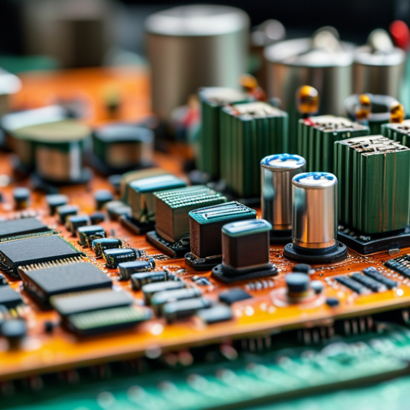
Identify the source before changing components. In a switching converter, rapid voltage changes create electric-field noise, while current changes create magnetic-field noise. The hottest areas are usually the switching node, diode loop, transformer winding, and gate-drive loop.
According to CISPR 32, radiated-emission testing commonly begins at 30 MHz, where small layout defects can become visible. IEC 61000-4-4 also uses 5/50 nanosecond electrical fast transients, showing how quickly unwanted energy can travel.
Trace both paths. Conducted EMI moves through input cables, output cables, ground planes, and parasitic capacitance. Radiated EMI leaves through large copper loops, heat sinks, enclosures, and unshielded wires.
Use a short, tight commutation loop. Reduce dv/dt with a controlled gate resistor or snubber. Reduce di/dt by minimizing stray inductance. Place ceramic bypass capacitors directly beside switching pins.
Add common-mode chokes only after measuring the noise path. Otherwise, they may hide the real problem. Keep sensitive feedback traces away from power nodes. Separate noisy and quiet return currents.
Use a continuous reference plane where possible. Shielding can help, but poor bonding often makes it worse. A near-field probe, current probe, and spectrum analyzer reveal more than visual inspection alone.
Small mistakes remain common, especially when the prototype differs from the final enclosure.
A compact power circuit can still radiate strongly when its current loops are large. Keep the switching node short, wide, and isolated from signal traces. Place the controller, transistor, diode, and input capacitor close together. The capacitor should sit directly across the high-current path. Every extra millimeter adds parasitic inductance.
Use a continuous reference plane beneath sensitive traces. Avoid routing feedback lines beside the switching node. If they must cross, use a ground-referenced layer and keep the crossing brief. International Electrotechnical Commission guidance in CISPR 16-1-1 shows why controlled measurement geometry matters: small changes in cable position can alter measured emissions significantly. Layout must control geometry before testing begins.
Reduce magnetic coupling by shrinking the hot-loop area. IEEE Transactions on Electromagnetic Compatibility studies commonly report substantial field reduction when loop dimensions decrease, although results depend on frequency, current, and board structure. A 2023 IPC design survey also identified return-path control as a recurring EMC weakness in power electronics. That matches practical bench work. I still find overlooked return currents after the schematic appears correct. It is an imperfect process. Probe the board near the switch node, capacitor, and connector. A few centimeters of unintended copper can become an antenna. Keep connector pins away from noisy planes, and add stitching vias around sensitive regions. Test early, because late shielding can hide a poor layout rather than fix it.
| No. | Layout Method | Recommended Implementation | Why It Reduces EMI | Practical Design Target | Verification Method |
|---|---|---|---|---|---|
| 1 | Minimize the High-Current Switching Loop | Place the power switch, rectifier or synchronous switch, and input or commutation capacitor as close together as possible. Route the forward and return conductors next to each other on the same layer whenever practical. | A smaller loop area produces less magnetic-field radiation because the loop captures and radiates less electromagnetic flux during rapid current changes. | Keep the critical switching loop compact and avoid unnecessary vias, long traces, and branch connections. | Inspect the current path and compare near-field probe scans before and after routing changes. |
| 2 | Place High-Frequency Decoupling Capacitors Close to the Device | Position the smallest, lowest-inductance ceramic capacitor directly between the device supply and its return path. Use short, wide connections and avoid routing the capacitor through a distant via pair. | Local decoupling supplies fast current pulses and prevents high-frequency current from spreading through larger power and ground planes. | Keep the capacitor connection short, direct, and free of narrow neck-downs; use multiple vias when a layer transition is required. | Measure supply ringing with a short-ground-spring oscilloscope probe at the device pins. |
| 3 | Provide a Continuous, Low-Impedance Return Path | Use an uninterrupted reference plane beneath fast signal and switching paths. Avoid slots, voids, split planes, and unnecessary plane transitions under high-frequency routes. | High-frequency current follows the path of lowest impedance, which is usually directly beneath the associated signal trace. Interruptions force return current to spread or detour, increasing radiated coupling. | Maintain a continuous reference plane under fast nets and place stitching vias close to unavoidable layer transitions. | Review plane geometry in the layout tool and verify return-current continuity with field-solver or impedance analysis when available. |
| 4 | Separate Noisy Nodes from Sensitive Circuits | Keep switch nodes, gate-drive traces, inductors, transformers, and high-current copper away from analog inputs, clocks, reset lines, communication interfaces, and sensor traces. | Fast voltage transitions and high di/dt currents can couple into nearby circuits through electric fields, magnetic fields, shared impedance, and parasitic capacitance. | Define a quiet-zone boundary around sensitive circuitry and prevent high dv/dt copper from passing over or alongside sensitive traces. | Perform an aggressor-victim review and monitor sensitive-node noise while varying load current and switching frequency. |
| 5 | Control the Switch-Node Copper Area | Make the switch node large enough for current capacity and thermal requirements, but no larger. Do not route unrelated traces beneath or beside this high-voltage, fast-transition node. | The switch node combines high dv/dt with parasitic capacitance, making it a major source of common-mode displacement current and electric-field coupling. | Use the smallest practical switch-node area and keep it away from chassis, heat sinks, connectors, and sensitive reference planes. | Use near-field electric-field scans and inspect common-mode current on cables or external harnesses. |
| 6 | Route Gate-Drive and Control Traces Carefully | Keep gate-drive traces short, route the gate and source or emitter return together, and place the gate resistor near the controlled device. Keep control traces away from the switch node and power loop. | A compact gate loop reduces ringing and limits unintended gate voltage caused by parasitic inductance. Controlled switching also reduces excessive high-frequency harmonics. | Use a dedicated gate-return path and tune the gate resistance only after checking switching loss, overshoot, and electromagnetic noise. | Measure gate-to-source or gate-to-emitter voltage directly at the device pins during turn-on and turn-off. |
| 7 | Use Layer Transitions, Stitching, and Filtering Strategically | Keep high-frequency paths on one layer when possible. When a transition is unavoidable, place adjacent return vias nearby. Add chassis or shield stitching at cable exits and locate filtering components at the enclosure or board entry point. | Short transition paths preserve return-current continuity, while controlled stitching and entry-point filtering reduce the distance over which common-mode noise can travel. | Keep filters at the noise boundary, minimize unfiltered trace length, and use multiple closely spaced stitching vias around shield or chassis interfaces. | Test conducted and radiated emissions with representative cables, enclosure configuration, load, and switching conditions. |
Reducing EMI from power devices often begins at the interfaces where noise escapes. Place a high-frequency decoupling capacitor directly beside each power pin. Keep the connection short, wide, and free from unnecessary vias. A small capacitor handles fast switching edges, while a larger capacitor supports slower load changes. Use both only when measurements justify them. More capacitance does not always mean less noise.
Filtering should also protect signal interfaces. Add a common-mode filter or ferrite element where cables leave the enclosure. Keep the filter close to the entry point, not beside the noisy switching node. Route filtered and unfiltered traces separately. Otherwise, noise can couple around the filter. On a test board, a long capacitor trace once created a visible ringing peak during load transients. The component value was acceptable. The layout was not. That mistake changed my review checklist.
Measure conducted noise at the input and output ports with consistent cable placement. Use a near-field probe to inspect the switching loop before changing components. A filter may reduce one frequency while increasing another. Check the complete spectrum. Signal-ground connections deserve equal attention. A narrow return path can turn a clean interface into an antenna. Keep reference planes continuous beneath sensitive traces. Small improvements matter. But every change should be verified under maximum load, startup, and rapid current transitions.
Apply filtering and decoupling at power and signal interfaces.
The chart shows the calculated impedance of representative 100 nF and 1 µF decoupling capacitors across frequency. Lower impedance generally provides a better high-frequency path for unwanted current, helping reduce noise at power and signal interfaces. The calculation uses Z = √(ESR² + (2πfL − 1/(2πfC))²) and includes realistic equivalent series resistance and inductance assumptions.
Practical EMI reduction also depends on minimizing current-loop area, placing capacitors close to device pins, using LC or π filters, selecting ferrite beads or common-mode chokes where appropriate, improving return-path continuity, separating noisy and sensitive traces, and adding suitable shielding and grounding.
7 Best Ways to Reduce EMI from Power Devices
Use shielding, grounding, and cable control as one containment system. A metal enclosure can block radiated noise, but only when seams, vents, and connectors remain electrically continuous. Conductive gaskets help. Paint around bonding points can quietly defeat them. I have seen a low-noise prototype fail because one painted mounting screw interrupted the return path.
Ground high-frequency currents with short, wide connections. Avoid long pigtail wires; their inductance increases impedance as frequency rises. Separate protective earth, signal reference, and noisy power returns where the design requires it. Add feedthrough filters at the enclosure boundary, not several centimeters inside. Keep filter leads short. That detail matters. FCC Part 15, Section 15.107, sets conducted-emission limits from 150 kHz to 30 MHz, while IEC 61000-4-6 tests immunity across 150 kHz to 80 MHz. These ranges show why apparently harmless cable layouts can become antennas.
Control every cable leaving the device. Minimize loop area, route power and return conductors together, and use twisted pairs for differential currents. Clamp ferrites near the noise source or enclosure entry, then verify their impedance at the actual switching frequency. Do not trust a datasheet curve alone. CISPR 32 testing distinguishes conducted and radiated emissions, so passing one measurement does not prove complete containment. A practical test uses a near-field probe, a spectrum analyzer, and repeated load conditions. My own weak point is assuming the quietest bench setup represents installation reality. It rarely does.
7 Best Ways to Reduce EMI from Power Devices
Reducing EMI starts with measurement, not guesswork. Build a repeatable test setup with a defined load, input voltage, cable position, and grounding method. Use a line impedance stabilization network, spectrum analyzer, near-field probe, and current probe where appropriate. Record switching harmonics, ringing frequency, peak amplitude, and test conditions. Compare these results with gate voltage and drain-current waveforms. This links visible noise to its physical source.
Seven design levers often work together: shrink high di/dt loops, place ceramic capacitors close to switching nodes, damp ringing with a snubber, control gate slew rate, separate power and signal returns, improve common-mode filtering, and strengthen shield bonding. Change one feature at a time. Otherwise, the result becomes difficult to trust. A filter may reduce conducted noise but increase voltage stress or move emissions into another frequency range. That trade-off needs review.
Tips: Keep it repeatable. Test one change per revision and retain the raw data. Use the same probe location and bandwidth settings every time. Inspect the prototype physically; a long capacitor lead or loose shield bond can defeat a carefully calculated design. In practice, early tests sometimes reveal an unexpected connector or heatsink path. That is useful evidence, not failure. Recheck the full operating range, because a quiet device at light load may become noisy during startup or peak current.
: Rapid voltage changes create electric-field noise. Rapid current changes create magnetic-field noise. The switching node, diode loop, transformer winding, and gate-drive loop need close inspection.
Conducted noise travels through input cables, output cables, ground planes, and parasitic capacitance. Radiated noise leaves through copper loops, heat sinks, enclosures, and unshielded wires. Large loops are common escape routes.
Keep high-current commutation loops short and tight. Minimize stray inductance to reduce current-change noise. Place ceramic capacitors directly beside switching pins. A neat schematic cannot rescue poor physical spacing.
A snubber can damp ringing around switching nodes. A controlled gate resistor can reduce excessive voltage-change speed. Measure the ringing frequency before selecting component values. More damping is not always better.
Place a small, high-frequency capacitor beside each power pin. Use short, wide connections with minimal unnecessary vias. A larger capacitor can support slower load changes. More capacitance does not always reduce EMI.
Put common-mode filters or ferrite components near cable entry points. Separate filtered traces from unfiltered traces. Keep sensitive feedback traces away from switching nodes. Noise can bypass a filter through nearby copper.
Use a near-field probe to scan switching loops and heat sinks. Use a current probe to inspect cable and return-current paths. A spectrum analyzer shows ringing peaks and harmonic energy. Visual inspection alone misses small but important defects.
Keep the load, input voltage, cable position, grounding, and probe settings consistent. Record ringing frequency, peak amplitude, switching harmonics, and operating conditions. Test startup, maximum load, and rapid current transitions. Light-load results can be misleading.
Change one feature per revision and retain the raw measurement data. Compare noise results with gate-voltage and drain-current waveforms. Check whether a filter reduces one frequency but increases another. A quieter prototype may still have higher component stress.
Reducing electromagnetic interference from power devices requires a systematic approach that addresses both the sources of noise and the paths through which it travels. Start by identifying switching nodes, high-current loops, fast voltage transitions, and unintended return paths that may generate or spread EMI. Improve the circuit layout by shortening current loops, separating noisy and sensitive sections, controlling trace spacing, and placing components to minimize electromagnetic coupling. Filtering and decoupling should also be applied at power and signal interfaces, using suitable components and carefully planned placement to suppress high-frequency noise before it enters or leaves the device.
Effective containment further depends on appropriate shielding, grounding, and cable control. Enclosures, ground connections, and cable routing should be designed to prevent radiation and reduce common-impedance coupling. Finally, test EMI performance under realistic operating conditions, locate the dominant problems, and refine the design through repeated measurements. By combining source identification, layout optimization, filtering, containment, and verification, engineers can reduce electromagnetic interference from power devices while improving reliability, compliance, and overall system performance.

JDI Power Supply